
LOCTITE ABLESTIK ABP 8068TA
Harmonization Code : 3506.91.90.99 | Prepared glues and other prepared adhesives, not elsewhere specified or included; products suitable for use as glues or adhesives, put up for retail sale as glues or adhesives, not exceeding a net weight of 1 kg ; Adhesives based on polymers of headings 3901 to 3913 or on rubber; Other ; Other

Main features
- Excellent workability
- Dispensable
- Printable
Product Description
LOCTITE ABLESTIK ABP 8068TA is a semi-sintering die attach adhesive designed for semiconductor packages requiring high thermal and electrical conductivity. This material’s epoxy assisted sintering formulation is designed to provide high adhesion, high thermal and low stress properties which are essential for thermal and reliability performances of high end power packages. .
LOCTITE ABLESTIK ABP 8068TA has a thermal performance that is comparable to a solder paste material. In conventional box oven curing, it will cure at 1 hour at 200ºC or 175ºC. This silver filled conductive adhesive is printable and dispensable with excellent workability. It offers good sintering properties when used on Ag, PPF, Au and Cu substrates with a high thermal stability. Its high reliability make it a good solder replacement candidate and is typically used for packages such as QFN, LGA and HBLED.
Packaging
TDS, SDS & Technical Documents
- LOCTITE ABLESTIK ABP 8068TA
- LOCTITE ABLESTIK ABP 8068TA
- MSDS 2314652 en_GB
- 8068 TA Printability test
Technical Specifications
General Properties
Thermal Properties
Chemical Properties
Physical Properties
Additional Information
How would this perform for GaN on SiC to Au plated Cu?
Silicon Nitride is an alternative to Silicon. The wafer / chip is normally fabricated from Silicon Nitride. This is mechanically fairly similar to silicon (it’s a bit harder & more brittle), so die attach that works with silicon is typically good on SiN.
GaN (Gallium Nitride) is a semiconductor layer that is grown on top of a silicon or SiN wafer / chip surface. So for die attach it is similar to attaching a Si or SiN chip.
8068TA is a “semi-sinter” material. It needs a layer of Ag or Au on both the chip & the substrate to give a good bond. An SiC wafer should have a metal back side metallization (BSM) like Ag or Au and this is the surface to sinter to. Bare Cu can also be OK for some “non-critical” applications, but it is not recommended.
Cure Schedule
For die size <5 x 5 mm
- 20 minutes ramp from 25°C to 130°C, hold for 30 to 60 minutes; 15 minutes ramp to 200°C, hold for 60 minutes in N2 or air oven
For die size >5 x 5 mm
- 20 minutes ramp from 25°C to 130°C, hold for 120 minutes; 15 minutes ramp to 200°C, hold for 60 minutes in N2 or air oven
Alternate Cure Schedule
Suitable for Ag, Au and PPF substrates
- 20 minutes ramp from 25°C to 130°C, hold for 30 minutes; 10 minutes ramp to 175°C, hold for 60 minutes in N2 or air oven
Recently viewed products
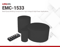
LINQSOL EMC-1533 | Black Epoxy Molding Compound
- Green molding compound
- Designed for transistor outline (TO) and double decawatt (D2PAK) packages
- Excellent workability, low water absorption, low modulus, and excellent thermal stability
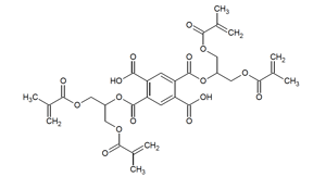
A675-100 | PMDGM adhesion promoter Additive
- Versatile
- Adhesion promoter
- Pyromellitic Dianhydride Glycerol Dimethacrylate Adduct
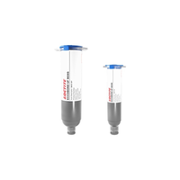
LOCTITE ECCOBOND UF8830S
- High purity
- Improved toughness
- Good flow with self filleting

HT 10000-R | One part Hybrid Thermal Gel
- Dark Gray
- 10 Thermal Conductivity
- Good dispense rate

SAC125N | PbFree Solder Spheres
- Lead-Free Solder Spheres
- Lowest cost Sn/Ag/Cu Alloy
- Nickel Dopped, hence the SACNi name
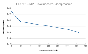
LINQCELL GDP210-MP | 210um Carbon Paper
- 0.21mm - 210um - 8.2mil
- Treated at 1600°C
- With MPL and Hydrophobic coating


